 English
 العربية
 bosanski jezik
 Български
 Català
 粤语
粤语 中文(漢字)
 Hrvatski
 Čeština
 Dansk
Dansk Nederlands
 Eesti keel
 Suomi
Suomi Français
 Deutsch
 Ελληνικά
 עברית
עברית Magyar
 Italiano
 日本語
日本語 한국어
한국어 Latviešu valoda
 Bahasa Melayu
 Norsk
Norsk پارسی
پارسی Polski
 Português
 Română
 Русский
 Cрпски језик
 Slovenčina
 Slovenščina
 Español
 Svenska
 தமிழ்
தமிழ் ภาษาไทย
 Tiếng Việt
Key points of electrical and signal harness manufacturing process
1. Design stage
Requirement analysis and parameter definition
According to the functional requirements of the equipment, clarify the parameters such as electrical performance, mechanical strength, temperature resistance and anti-interference ability of the harness.
Signal harnesses need to consider signal transmission stability and use shielding layer, twisted pair or coaxial cable design.
Drawings and process file preparation
Draw the harness layout diagram and mark the wire length, wire diameter, color coding and connector type.
Automatically generate process files through modeling design software (such as MBD) to reduce manual intervention.
Easy to install, maintain, and ensure electrical equipment Wire Harness Manufacturing
The process begins with a design phase where engineers determine the harness’s specifications, including the number of wires, connecteurs, and overall routing.
This phase often involves using specialized software to create a detailed design of the harness.
Prototyping:
A prototype may be created to test the design and make any necessary adjustments before mass production.
2. Material preparation and pretreatment
Raw material screening and inspection
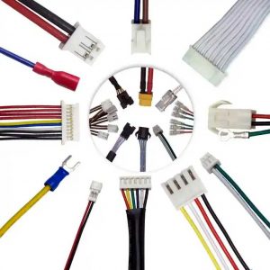
The wire material (cuivre, alloy, etc.) must meet the conductivity and corrosion resistance requirements, and the connector must pass the contact resistance test.
Signal harnesses give priority to low-loss insulating materials (such as FEP, Ptfe).
Wire cutting and stripping
The wire cutting machine cuts the wire according to the preset length, and the error is controlled within ±0.5mm. The end face must be flat and free of burrs.
The stripping length must accurately match the terminal crimping requirements to avoid damaging the conductor.
Fabricant de harnais de fil professionnel_electrical, Signal, Harnais de fil électronique
3. Terminal crimping and riveting
Crimping process
Adjust the crimping machine parameters (pressure, stroke) to ensure that the terminal and the wire are tightly connected, and verify the strength through a tensile test after crimping.
The signal terminal is gold-plated/silver-plated to reduce contact resistance and oxidation risk.
Riveting device application
Automated equipment (such as patent CN 222785620 U) achieves terminal clamping and fixation through a linkage mechanism to reduce manual operation errors.
How Additive Manufacturing Can Improve Wire Harness Assembly
4. Assembly and molding
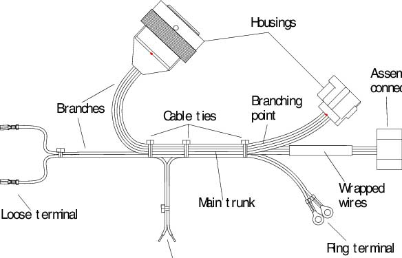
Wiring binding
Lay out the wires according to the positioning plate, and bind them in sections to avoid cross interference.
Install corrugated tubes or heat shrink tubing at key locations to improve mechanical protection and insulation performance.
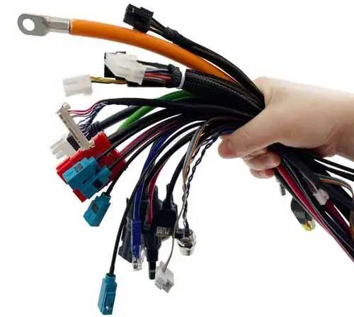
Connector assembly
Clean the terminal contact surface before inserting the PIN to ensure a stable plug-in; the signal connector needs to be treated with anti-static.
V. Testing and Verification
Electrical Performance Test
Conductivity test: Check the continuity and short circuit of the line.
Withstand voltage test: Verify the withstand voltage of the insulation layer (such as 500V/1min).
Signal integrity detection
High-frequency signal harnesses need to test crosstalk, attenuation and impedance matching (such as TDR test).
VI. Special process optimization
Injection molding
The signal harness connector adopts injection molding process to achieve sealing and anti-vibration design.
Mise à niveau de l'automatisation
Introduce processes such as robot-assisted wiring and laser marking to improve efficiency and consistency.
Key equipment and technology patents Riveting device: The terminal clamping and riveting are completed synchronously through the linkage mechanism to reduce the time-consuming process.
Multi-layer PCB process: Used for circuit integration of complex harnesses (such as CN115103531B patent).
The above process integrates design, matériels, processing, testing and other aspects, taking into account the versatility and special needs of signal harnesses to ensure that the product meets electrical and signal transmission standards.